Main MCU Firmware
Tools
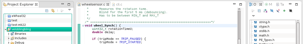
Kinetis Design Studio Integrated Development Environment (IDE)
The Kinetis Design Studio (KDS)Processor Expert Software and Embedded Components
Processor Expert Software(ARCHIVED) USB Stack
Debug Adapter
The KDS supports following adapters (protocols):- OpenSDA
 Serial and Debug Adapter (proprietary Freescale/NXP/P&E Microcomputer Systems)
- Segger (industrial standard)
- OpenOCD,
3.2.1 Debug interface Signals with SPI and GPIO capability are used to connect directly to the SWD of the K22F. These signals are also brought out to a standard 10-pin (0.05) Cortex debug connector (J11). It is possible to isolate the K22F MCU from the OpenSDAv2 circuit and use J11 to connect to an off-board MCU. To accomplish this, cut the trace on the bottom side of the PCB that connects J7 pin 2 to J11 pin 4. This will disconnect the SWD_CLK pin to the K22F so that it will not interfere with communication to an off-board MCU connected to J7. The J11 header is populated by default. A mating cable, such as a Samtec FFSD IDC cable, can then be used to connect from the OpenSDAv2 of the FRDM-K22F to an off-board SWD connector.You can still use the FRDM-K22F as a prototype board. You should solder a pinheader and plug a jumper if you want to use the FRDM-K22F as a prototype board. See also an excellent introduction to OpenOCD/CMSIS-DAP Debugging
Get the Software and Import it into the IDE
Get the Source from the Repository
The Velo Bling-Bling Kinetis project is on the GitHub repository https://github.com/spyren/veloblingbling-mcupsi@homer:~/veloblingbling> git clone https://github.com/spyren/veloblingbling-mcu Klone nach 'veloblingbling-mcu' ... remote: Counting objects: 265, done. remote: Compressing objects: 100% (97/97), done. remote: Total 265 (delta 167), reused 260 (delta 166), pack-reused 0 Empfange Objekte: 100% (265/265), 223.50 KiB | 0 bytes/s, Fertig. Löse Unterschiede auf: 100% (167/167), Fertig. Prüfe Konnektivität ... Fertig. psi@homer:~/veloblingbling>
Import the Project into the IDE
File -> Import -> General -> Existing Projects into Workspace ->MCU MK22DX256VLF5
- Data sheets
- K22_50: Next-Generation Kinetis K22 USB 50 MHz MCUs
- MK22DX256VLF5 Data Sheet 48 Pin
- K22 Sub-Family Reference Manual MK22DX128VLF5, MK22DX256VLF5
- K22_50: Next-Generation Kinetis K22 USB 50 MHz MCUs
- Features
- Core ARM Cortex M4, 50 MHz
- Run mode current 17 mA, wait 8 mA
- A/D Converter - Bits (bit) 16
- Additional Features Vref
- Ambient Operating Temperature (Min-Max) (°C) -40 to 105
- Analog Comparator 2
- Cache (kB) 0
- Debug Features JTAG, Serial Wire Debug, cJTAG
- EEPROM (kB) 4
- External Bus Interface n/a
- FlexMemory (KB) 64
- I/O Pins 29
- Independent ADC modules 1
- Internal Flash (kB) 256
- Internal RAM (kB) 32
- Max Simultaneous ADC channels 1 DP14 SE
- Pulse Width Modulators - Channels 10
- Sample Exception Availability Y
- Serial Interface - Number of Interfaces 4
- Serial Interface - Type UART, SPI, I2C, I2S
- USB OTG LS/FS
- Supply Voltage (Min-Max) (V) 1.71 to 3.6
- Timer type Low Power Timer, Periodic Interrupt Timer, Programmable Delay Block
- Total DMA Channels 16
- Total Flash memory (kB) 320
- LQFP-48
Comments


| I | Attachment | History | Action | Size | Date | Who | Comment |
|---|---|---|---|---|---|---|---|
| |
kinetisdesignstudio.png | r1 | manage | 71.8 K | 2016-03-30 - 20:27 | PeterSchmid |
Topic revision: r6 - 2016-04-23 - PeterSchmid


Ideas, requests, problems regarding TWiki? Send feedback