Difference: BoardSupportPackageH743 (1 vs. 13)
Revision 132022-06-30 - PeterSchmid
Revision 122022-06-30 - PeterSchmid
| Line: 1 to 1 | ||||||||
|---|---|---|---|---|---|---|---|---|
%DASHBOARD{ section="banner" | ||||||||
| Line: 74 to 74 | ||||||||
| EXTImod ( u a -- ) Sets for pin a (D11, D12, D13) the EXTI mode u: 0 rising, 1 falling, 2 both edges, 3 none EXTIwait ( u a -- ) Wait for EXTI interrupt on pin a (D11, D12, D13), timeout u in [ms] | ||||||||
| Changed: | ||||||||
| < < | pwmpin! ( u a -- ) sets the digital output port pin a (D5=5, D6=6, D9=9, D10=10, D14=14, and D15=15) to a PWM value u (0..1000). | |||||||
| > > | pwmpin! ( u a -- ) sets the digital output port pin a (D3=3, D4=4, D5=5, D6=6, D9=9, and D10=10) to a PWM value u (0..1000). | |||||||
| Default frequency is 1 kHz, TIMER3/TIMER4 pwmprescale ( u -- ) Sets the PWM prescale for TIMER3/TIMER4. 42 kHz / prescale, default 42 -> PWM frequency 1 kHz | ||||||||
Revision 112022-06-30 - PeterSchmid
| Line: 1 to 1 | ||||||||
|---|---|---|---|---|---|---|---|---|
%DASHBOARD{ section="banner" | ||||||||
Revision 102022-06-28 - PeterSchmid
| Line: 1 to 1 | ||||||||
|---|---|---|---|---|---|---|---|---|
%DASHBOARD{ section="banner" | ||||||||
| Line: 25 to 25 | ||||||||
| ||||||||
| Changed: | ||||||||
| < < |
| |||||||
| > > |
| |||||||
| ||||||||
| Line: 34 to 34 | ||||||||
| ||||||||
| Changed: | ||||||||
| < < |
| |||||||
| > > |
| |||||||
| ||||||||
Revision 92022-06-27 - PeterSchmid
| Line: 1 to 1 | ||||||||
|---|---|---|---|---|---|---|---|---|
%DASHBOARD{ section="banner" | ||||||||
| Line: 6 to 6 | ||||||||
| title="Board Support Package for the STM NUCLEO-H743ZI Board" titlestyle="color:#F00000;" }% | ||||||||
| Changed: | ||||||||
| < < | Intro
| |||||||
| > > | Intro
| |||||||
| DRAFT
The board support package for the STM NUCLEO-H743ZI | ||||||||
| Changed: | ||||||||
| < < | Contents
| |||||||
| > > | Contents
| |||||||
| ||||||||
| Changed: | ||||||||
| < < |
| |||||||
| > > |
| |||||||
| ||||||||
Revision 82022-06-24 - PeterSchmid
| Line: 1 to 1 | ||||||||
|---|---|---|---|---|---|---|---|---|
%DASHBOARD{ section="banner" | ||||||||
| Line: 536 to 536 | ||||||||
SD Card / SDIO Pins | ||||||||
| Changed: | ||||||||
| < < | SDIO_D0 / PC8 (internal) / CN8.2SDIO_D1 / PC9 (internal) / CN8.4SDIO_D2 / PC10 (internal) / CN8.6SDIO_D3 / PC11 (internal) / CN8.8SDIO_CLK / PC12 (internal) / CN8.10SDIO_CMD / PD2 (internal) / CN8.12SD_DETECT / PB12 (internal) / optional / CN7.7 | |||||||
| > > | SDIO_D0 / DATA_OUT / PC8 (internal) / CN8.2SDIO_D1 / DAT1 / PC9 (internal) / CN8.4SDIO_D2 / DAT2 / PC10 (internal) / CN8.6SDIO_D3 / CS / PC11 (internal) / CN8.8SDIO_CLK / SCLK /PC12 (internal) / CN8.10SDIO_CMD / DATA_IN / PD2 (internal) / CN8.12SD_DETECT / CARD_DETECT / PB12 (internal) / optional / CN7.7 | |||||||
QSPI | ||||||||
Revision 72022-06-22 - PeterSchmid
| Line: 1 to 1 | ||||||||
|---|---|---|---|---|---|---|---|---|
%DASHBOARD{ section="banner" | ||||||||
| Line: 25 to 25 | ||||||||
| ||||||||
| Changed: | ||||||||
| < < |
| |||||||
| > > |
| |||||||
| ||||||||
| Line: 545 to 545 | ||||||||
SD_DETECT / PB12 (internal) / optional / CN7.7 | ||||||||
| Added: | ||||||||
| > > | QSPIQS_CS / PG6 (external) / CN10.13QS_CLK / PB2 (external) / CN10.15QS_D3 / PD13 (external) / CN10.19QS_D1 / PD12 (external) / CN10.21QS_D0 / PD11 (external) / CN10.23QS_D2 / PE2 (external) / CN10.25 | |||||||
USBUSB_DP / PA12USB_DM / PA11 | ||||||||
Revision 62022-06-19 - PeterSchmid
| Line: 1 to 1 | ||||||||
|---|---|---|---|---|---|---|---|---|
| Changed: | ||||||||
| < < |
| |||||||
| > > |
| |||||||
|
%DASHBOARD{ section="banner" | ||||||||
| Changed: | ||||||||
| < < | image="/twiki/pub/MecrispCube/MecrispCubeH7/NUCLEO-H743ZI2-header.jpg" | |||||||
| > > | image="/twiki/pub/MecrispCube/MecrispCubeH74x/NUCLEO-H743ZI2-header.jpg" | |||||||
| title="Board Support Package for the STM NUCLEO-H743ZI Board" titlestyle="color:#F00000;" }% | ||||||||
| Line: 418 to 418 | ||||||||
| Changed: | ||||||||
| < < | Error: (1) can't find pinout_legend_2017-06-28-2.png at /MecrispCube.MecrispCubeH7 | |||||||
| > > |  | |||||||
| Changed: | ||||||||
| < < | Error: (1) can't find nucleo_h743zi2_zio_left_2019_10_9.png at /MecrispCube.MecrispCubeH7 Error: (1) can't find nucleo_h743zi2_zio_right_2019_10_9.png at /MecrispCube.MecrispCubeH7 Error: (1) can't find nucleo_h743zi2_morpho_left_2019_10_9.png at /MecrispCube.MecrispCubeH7 Error: (1) can't find nucleo_h743zi2_morpho_right_2019_10_9.png at /MecrispCube.MecrispCubeH7 | |||||||
| > > |     | |||||||
SCL D15, SDA D14 | ||||||||
Revision 52022-06-18 - PeterSchmid
| Line: 1 to 1 | ||||||||
|---|---|---|---|---|---|---|---|---|
| Changed: | ||||||||
| < < |
| |||||||
| > > |
| |||||||
|
%DASHBOARD{ section="banner" | ||||||||
| Changed: | ||||||||
| < < | image="/twiki/pub/MecrispCube/MecrispCubeH743/NUCLEO-H743ZI2-header.jpg" | |||||||
| > > | image="/twiki/pub/MecrispCube/MecrispCubeH7/NUCLEO-H743ZI2-header.jpg" | |||||||
| title="Board Support Package for the STM NUCLEO-H743ZI Board" titlestyle="color:#F00000;" }% | ||||||||
| Line: 418 to 418 | ||||||||
| Changed: | ||||||||
| < < | Error: (1) can't find pinout_legend_2017-06-28-2.png at /MecrispCube.MecrispCubeH743 | |||||||
| > > | Error: (1) can't find pinout_legend_2017-06-28-2.png at /MecrispCube.MecrispCubeH7 | |||||||
| Changed: | ||||||||
| < < | Error: (1) can't find nucleo_h743zi2_zio_left_2019_10_9.png at /MecrispCube.MecrispCubeH743 Error: (1) can't find nucleo_h743zi2_zio_right_2019_10_9.png at /MecrispCube.MecrispCubeH743 Error: (1) can't find nucleo_h743zi2_morpho_left_2019_10_9.png at /MecrispCube.MecrispCubeH743 Error: (1) can't find nucleo_h743zi2_morpho_right_2019_10_9.png at /MecrispCube.MecrispCubeH743 | |||||||
| > > | Error: (1) can't find nucleo_h743zi2_zio_left_2019_10_9.png at /MecrispCube.MecrispCubeH7 Error: (1) can't find nucleo_h743zi2_zio_right_2019_10_9.png at /MecrispCube.MecrispCubeH7 Error: (1) can't find nucleo_h743zi2_morpho_left_2019_10_9.png at /MecrispCube.MecrispCubeH7 Error: (1) can't find nucleo_h743zi2_morpho_right_2019_10_9.png at /MecrispCube.MecrispCubeH7 | |||||||
SCL D15, SDA D14 | ||||||||
Revision 42022-04-18 - PeterSchmid
| Line: 1 to 1 | ||||||||
|---|---|---|---|---|---|---|---|---|
%DASHBOARD{ section="banner" | ||||||||
| Line: 22 to 22 | ||||||||
| ||||||||
| Changed: | ||||||||
| < < |
| |||||||
| > > |
| |||||||
| ||||||||
| Line: 30 to 30 | ||||||||
| ||||||||
| Changed: | ||||||||
| < < |
| |||||||
| > > |
| |||||||
| ||||||||
| Changed: | ||||||||
| < < |
| |||||||
| > > |
| |||||||
| ||||||||
| Line: 467 to 468 | ||||||||
D7 / PC13 / CN10.2 | ||||||||
| Added: | ||||||||
| > > |
| |||||||
| ||||||||
| Line: 493 to 495 | ||||||||
D13 / SCK / PA5 / CN7.10
| ||||||||
| Changed: | ||||||||
| < < |
| |||||||
| > > |
| |||||||
D14 / SDA / PB9 / CN7.4 | ||||||||
| Line: 511 to 513 | ||||||||
A0 / D16 / PA3 / CN9.1
| ||||||||
| Changed: | ||||||||
| < < |
| |||||||
| > > |
| |||||||
A1 / D17 / PC0 / CN9.3 | ||||||||
| Line: 526 to 528 | ||||||||
A4 / D20 / PC2 / CN9.9 | ||||||||
| Changed: | ||||||||
| < < |
| |||||||
| > > |
| |||||||
A5 / D21 / PF10 / CN9.11
| ||||||||
| Line: 550 to 552 | ||||||||
VCP UARTSTLK_VCP_TX / PG14 / ST-LINK VCP Rx | ||||||||
| Changed: | ||||||||
| < < |
| |||||||
| > > |
| |||||||
STLK_VCP_RX / PG9 / ST-LINK VCP Tx | ||||||||
| Changed: | ||||||||
| < < |
| |||||||
| > > |
| |||||||
Revision 32022-03-08 - PeterSchmid
| Line: 1 to 1 | ||||||||
|---|---|---|---|---|---|---|---|---|
%DASHBOARD{ section="banner" | ||||||||
| Line: 20 to 20 | ||||||||
| ||||||||
| Changed: | ||||||||
| < < |
| |||||||
| > > |
| |||||||
| ||||||||
| Line: 39 to 41 | ||||||||
| ||||||||
| Changed: | ||||||||
| < < |
| |||||||
| > > |
| |||||||
| ||||||||
| Changed: | ||||||||
| < < | Defaults: Digital port pins D1, D5, D6, D9 to D13 are inputs; D0 (UART_RX) is input with 100 kOhm pull-up resistor; D14 (SDA) and D15 (SCL) are open drain outputs with 10 kOhm pull-up resistors; D5, D6, and D9 with internal pull-ups (for the push buttons). | |||||||
| > > | Defaults:
| |||||||
|
| ||||||||
| Line: 541 to 547 | ||||||||
USB_DP / PA12USB_DM / PA11 | ||||||||
| Added: | ||||||||
| > > | VCP UARTSTLK_VCP_TX / PG14 / ST-LINK VCP Rx
STLK_VCP_RX / PG9 / ST-LINK VCP Tx
| |||||||
Revision 22022-03-07 - PeterSchmid
| Line: 1 to 1 | ||||||||
|---|---|---|---|---|---|---|---|---|
%DASHBOARD{ section="banner" | ||||||||
| Line: 431 to 431 | ||||||||
RESET / JP1.16 | ||||||||
| Changed: | ||||||||
| < < | D0 / UART_RX / PB11 / JP1.3
| |||||||
| > > | D0 / UART_RX / PB7 / CN10.16
| |||||||
| Changed: | ||||||||
| < < | D1 / UART_TX / PB10 / JP1.2
D2 /SCK / PB13 / JP1.6
D3 / MISO / PB14 / JP1.4
| |||||||
| > > | D1 / UART_TX / PB6 / CN10.14
| |||||||
| Changed: | ||||||||
| < < | D4 / MOSI / PB15 / JP1.5
| |||||||
| > > | D2 / PG14 / CN10.12
| |||||||
| Changed: | ||||||||
| < < | D5 / Button C / PC7 / JP3.10
| |||||||
| > > | D3 / PE13 / CN10.10
| |||||||
| Changed: | ||||||||
| < < | D6 / Button B / PC6 / JP3.9
| |||||||
| > > | D4 / PE14 / CN10.8
| |||||||
| Changed: | ||||||||
| < < | D7 / PC13 | |||||||
| > > | D5 / PE11 / CN10.6
| |||||||
| Changed: | ||||||||
| < < | D8 / PC0 | |||||||
| > > | D6 / PE9 / CN10.4
| |||||||
| Added: | ||||||||
| > > | D7 / PC13 / CN10.2
| |||||||
| Deleted: | ||||||||
| < < | D9 / PB8 / JP3.8
| |||||||
| Changed: | ||||||||
| < < | D10 / PB9 / JP3.7 | |||||||
| > > | D8 / PF3 / CN7.20
D9 / PD15 / CN7.18 | |||||||
| ||||||||
| Changed: | ||||||||
| < < |
| |||||||
| > > |
| |||||||
| Changed: | ||||||||
| < < | D11 / PC3 / JP3.6
| |||||||
| > > | D10 / PD14 / CN7.16
| |||||||
| Changed: | ||||||||
| < < | D12 / PC2 / JP3.5
| |||||||
| > > | D11 / MOSI / PB5 / CN7.14
D12 / MISO / PA6 / CN7.12
| |||||||
| ||||||||
| Changed: | ||||||||
| < < | D13 / PC1 / JP3.4 | |||||||
| > > | D13 / SCK / PA5 / CN7.10
D14 / SDA / PB9 / CN7.4D15 / SCL / PB8 / CN7.2 | |||||||
| Deleted: | ||||||||
| < < | D14 / SDA / PB7 / JP3.12 | |||||||
| Changed: | ||||||||
| < < | D15 / SCL / PB6 / JP3.11 | |||||||
| > > | Analog Pins | |||||||
| Added: | ||||||||
| > > | A0 / D16 / PA3 / CN9.1
| |||||||
| Changed: | ||||||||
| < < | Analog Pins | |||||||
| > > | A1 / D17 / PC0 / CN9.3
| |||||||
| Changed: | ||||||||
| < < | A0 / GPIO 16 / PA4 / JP1.12
A1 / GPIO 17 / PA5 / JP1.11
A2 / GPIO18 / PA6 / JP1.10
| |||||||
| > > | A2 / D18 / PC3 / CN9.5
| |||||||
| Changed: | ||||||||
| < < | A3 / GPIO19 / PA7 / JP1.9
| |||||||
| > > | A3 / D19 / PB1 / CN9.7
| |||||||
| ||||||||
| Changed: | ||||||||
| < < | A4 / GPIO20 / PC4 / JP1.8
| |||||||
| > > | A4 / D20 / PC2 / CN9.9
| |||||||
| Changed: | ||||||||
| < < | A5 / GPIO21 / PC5 / JP1.7
| |||||||
| > > | A5 / D21 / PF10 / CN9.11
| |||||||
SD Card / SDIO Pins | ||||||||
| Changed: | ||||||||
| < < | SDIO_D0 / SD_MISO / PC8 (internal)SDIO_D1 / PC9 (internal)SDIO_D2 / PC10 (internal)SDIO_D3 / SD_CS / PC11 (internal)SDIO_CLK / SD_CLK / PC12 (internal)SDIO_CMD / SD_MOSI / PD2 (internal)SD_DETECT / PB12 (internal) | |||||||
| > > | SDIO_D0 / PC8 (internal) / CN8.2SDIO_D1 / PC9 (internal) / CN8.4SDIO_D2 / PC10 (internal) / CN8.6SDIO_D3 / PC11 (internal) / CN8.8SDIO_CLK / PC12 (internal) / CN8.10SDIO_CMD / PD2 (internal) / CN8.12SD_DETECT / PB12 (internal) / optional / CN7.7 | |||||||
USB | ||||||||
Revision 12022-03-07 - PeterSchmid
| Line: 1 to 1 | |||||||||||||||||||||||||||||||||||
|---|---|---|---|---|---|---|---|---|---|---|---|---|---|---|---|---|---|---|---|---|---|---|---|---|---|---|---|---|---|---|---|---|---|---|---|
| Added: | |||||||||||||||||||||||||||||||||||
| > > |
Board Support Package for the STM NUCLEO-H743ZI Board
Intro
DRAFT
The board support package for the STM NUCLEO-H743ZI
Contents
Overview
Board Support Words
led1! ( n -- ) sets LED1 (green)
led2! ( n -- ) sets LED2 (yellow)
led3! ( n -- ) sets LED3 (red)
led1@ ( -- n ) gets LED1 (green)
led2@ ( -- n ) gets LED2 (yellow)
led3@ ( -- n ) gets LED3 (red)
switch1? ( -- n ) gets switch1 (button A), closed=TRUE
dport! ( n -- ) sets the digital output port (D0=bit0 .. D15=bit15).
dport@ ( -- n ) gets the digital input/output port (D0=bit0 .. D15=bit15).
dpin! ( n a -- ) sets the digital output port pin a (D0=0 .. D15=15, A0=16 .. A6=23)
dpin@ ( a -- n ) gets the digital input/output port pin a
dmod ( u a -- ) sets the pin mode: 0 in, 1 in pull-up, 2 in pull-down, 3 out push pull, 4 out open drain,
5 out push pull PWM, 6 input capture, 7 output compare, 8 I2C, 9 USART, 10 analog
EXTImod ( u a -- ) Sets for pin a (D11, D12, D13) the EXTI mode u: 0 rising, 1 falling, 2 both edges, 3 none
EXTIwait ( u a -- ) Wait for EXTI interrupt on pin a (D11, D12, D13), timeout u in [ms]
pwmpin! ( u a -- ) sets the digital output port pin a (D5=5, D6=6, D9=9, D10=10, D14=14, and D15=15) to a PWM value u (0..1000).
Default frequency is 1 kHz, TIMER3/TIMER4
pwmprescale ( u -- ) Sets the PWM prescale for TIMER3/TIMER4. 42 kHz / prescale, default 42 -> PWM frequency 1 kHz
ICOCprescale ( u -- ) Sets the input capture / output compare prescale for TIMER2. default 42 -> 42 MHz / 42 = 1 MHz, timer resolution 1 us
ICOCperiod! ( u -- ) Sets the input capture / output compare (TIMER2) period. default $FFFFFFFF (4'294'967'295).
When the up counter reaches the period, the counter is set to 0.
For prescale 32 the maximum time is about 1 h 11 m
ICOCcount! ( -- u ) Sets the input capture / output compare counter for TIMER2
ICOCcount@ ( u -- ) Gets the input capture / output compare counter for TIMER2
ICOCstart ( -- ) Starts the ICOC period
ICOCstop ( -- ) Stops the ICOC period
OCmod ( u a -- ) Sets for pin a (D0, D1) the Output Compare mode u: 0 frozen, 1 active level on match,
2 inactive level on match, 3 toggle on match, 4 forced active, 5 forced inactive
OCstart ( u a -- ) Starts the output compare mode for pin a with pulse u
OCstop ( a -- ) Stops output compare for pin a
ICstart ( u -- ) Starts input capture u: 0 rising edge, 1 falling edge, 2 both edges
ICstop ( -- ) Stops input capture
waitperiod ( -- ) wait for the end of the TIMER2 period
OCwait ( a -- ) wait for the end of output capture on pin a
ICwait ( u -- u ) wait for the end of input capture with timeout u, returns counter u
apin@ ( a -- u ) gets the analog input port pin (A0=0 .. A6=6). Returns a 12 bit value (0..4095)
Using the Digital Port Pins (Input and Output)Set 8 port pins to push/pull output3 15 dmod \ set D15 (SCL) to Output 3 5 dmod \ set D5 to Output 3 6 dmod \ set D6 to Output 3 9 dmod \ set D9 to Output 3 10 dmod \ set D10 to Output 3 11 dmod \ set D11 to output 3 12 dmod \ set D12 to output 3 13 dmod \ set D13 to outputremap D15, D5, .. D13 create port-map 15 , 5 , 6 , 9 , 10 , 11 , 12 , 13 , : pin ( n -- n ) \ gets the Dx pin number cells port-map + @ ;
3 16 dmod \ set A0 to Output 3 17 dmod \ set A1 to Output 3 18 dmod \ set A2 to Output 3 19 dmod \ set A3 to Output 3 20 dmod \ set A4 to Output 3 21 dmod \ set A5 to output 3 2 dmod \ set D2 (SCK) to output 3 4 dmod \ set D4 (MOSI) to outputremap D15, D5, .. D13 create port-map 16 , 17 , 18 , 19 , 20 , 21 , 2 , 4 , Using the ADC (Analog Input Pins)Control the Neopixelapin@ ( a -- u ) returns the ADC value (12 bit, 0 .. 4095) from one of the analog pins A0 to A5 (0 .. 5). Here I use the A0 to control the neopixel blue led brightness.
: neo-blue ( -- )
  begin
0 apin@ 16 / neopixel!
10 osDelay drop
key? until
key drop
;
Control the Knightrider Paceapin@ ( a -- u ) returns the ADC value (12 bit, 0 .. 4095) from one of the analog pins A0 to A5 (0 .. 5). Here I use the A0 to control the delay.
Using the PWM (Analog Output Pins)Six port pins are supported so far. The 16 bit timers TIM3 (D5 and D6) and TIM4 (D9, D10, D14, and D15) are used for the timebase, time resolution is 1 us (42 MHz SysClk divided by 42). The PWM scale is from 0 (0 % duty cycle) to 1000 (100 % duty cycle), this results in a PWM frequency of 1 kHz. If you need higher PWM frequencies, decrease the divider and/or the scale. PWM port pins: D5 (TIM3CH2), D6 (TIM3CH1), D9 (TIM4CH3), D10 (TIM4CH4), D14 (TIM4CH2), and D15 (TIM4CH1). Simple test program to set brightness of a LED on pin D6 with a potentiometer on A0. Default PWM frequency is 1 kHz (prescaler set to 42). You can set the prescale with the wordpwmprescale from 42 kHz (value 1) down to 0.5 Hz (64000).
5 6 dmod   \ set D6 to PWM

: pwm ( -- )
  begin
    0 apin@  4 /  6 pwmpin!
    10 osDelay drop
    key?
  until
  key drop
;
Control an RC Servohttps://en.wikipedia.org/wiki/Servo_(radio_control
840 pwmprescale
5 5 dmod   \ set D5 to PWM

: servo ( -- )
  begin
    130 40 do
      i 5 pwmpin!
      i neopixel!
      i 40 = if
        1000 \ give some more time to get back
      else
        200
      then
      osDelay drop
    10 +loop
  key? until
  key drop
;
Using Input Capture and Output CompareTime BaseDefault timer resolution is 1 us. The 32 bit TIMER2 is used as time base for Input Capture / Output Compare. For a 5 s period 5'000'000 cycles are needed. All channels (input capture / output compare) use the same time base.
: period ( -- )
  5000000 ICOCperiod! \ 5 s period
  ICOCstart
  begin
     waitperiod
     cr .time
  key? until
  key drop
;
Output CompareOutput compare TIM2: D0, D1
7 0 dmod  \ output compare for D0
7 1 dmod  \ output compare for D1

: oc-toggle ( -- )
  5000000 ICOCperiod! \ 5 s period
  ICOCstart
  3 0 OCmod  1000000 0 OCstart \ toggle D0 after 1 s
  3 1 OCmod  2000000 1 OCstart \ toggle D1 after 2 s
  begin
     waitperiod
     cr .time
  key? until
  key drop
;
When you abort (hit any key) the program, the timer still runs and controls the port pins. To stop the port pins:
0 OCstop 1 OCstopOr change the prescale to make it faster or slower: 1 ICOCprescale Input CaptureThis sample program measures the time between the edges on port A1. if no event occurs within 2 seconds, "timeout" is issued. Hit any key to abort program.
: ic-test ( -- )
  6 17 dmod \ input capture on A1
  ICOCstart
  2 ICstart  \ both edges
  ICOCcount@ ( -- count )
  begin
    2000 \ 2 s timeout
    ICwait ( -- old-capture capture )
    cr
    dup 0= if
      ." timeout" drop
    else
      dup rot ( -- capture capture old-capture )
      - 1000 / . ." ms"
    then
  key? until
  key drop
  drop
  ICstop
;
Using EXTI lineD11, D12, and D13 can be used as an EXTI line. EXTIs are external interrupt lines, D13 uses EXTI1 (EXTI Line1 interrupt), D12 EXIT2, and D11 EXTI3.
: exti-test ( -- )
  2 11 EXTImod \ both edges on D11
  begin
    2000 11 EXTIwait \ wait for edge on D11 with 2 s timeout
    cr
    0= if
      11 dpin@ if
        ." rising edge"
      else
        ." falling edge"
      then
    else
      ." timeout"
    then
  key? until
  key drop
;
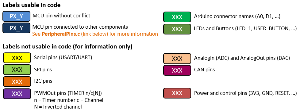
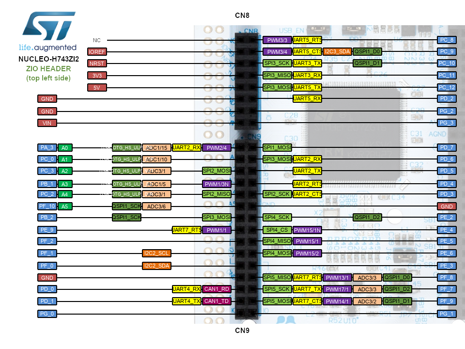
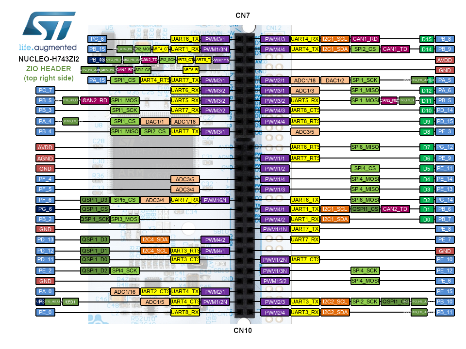
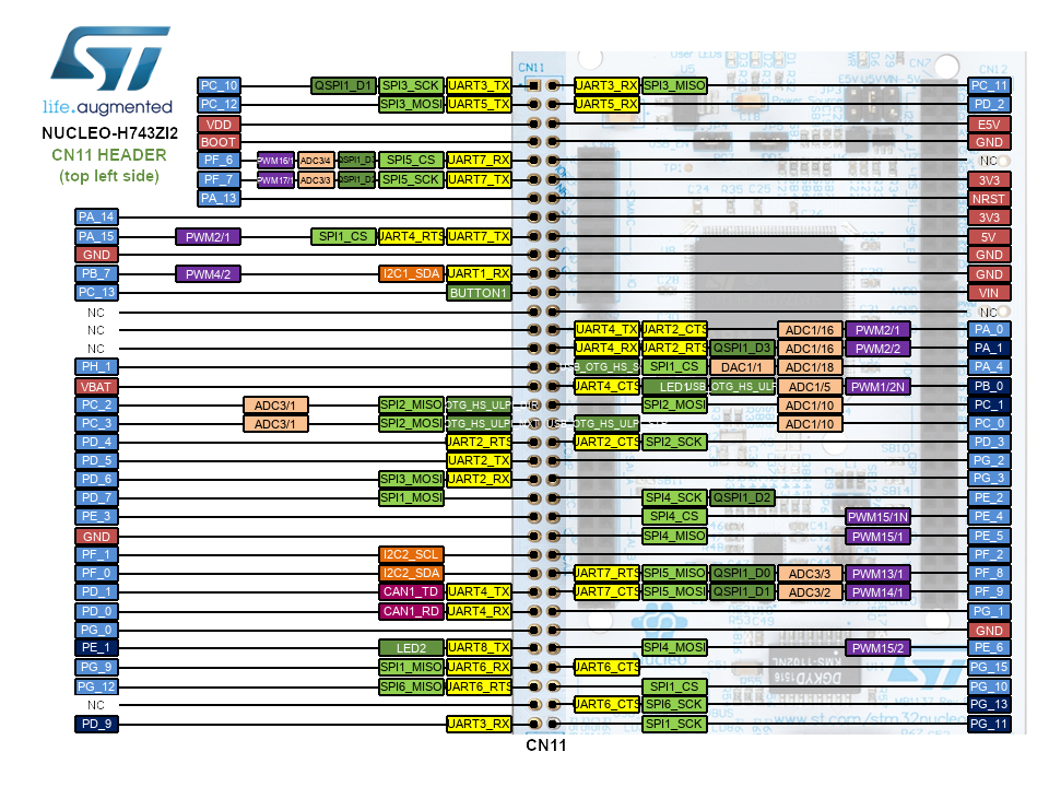
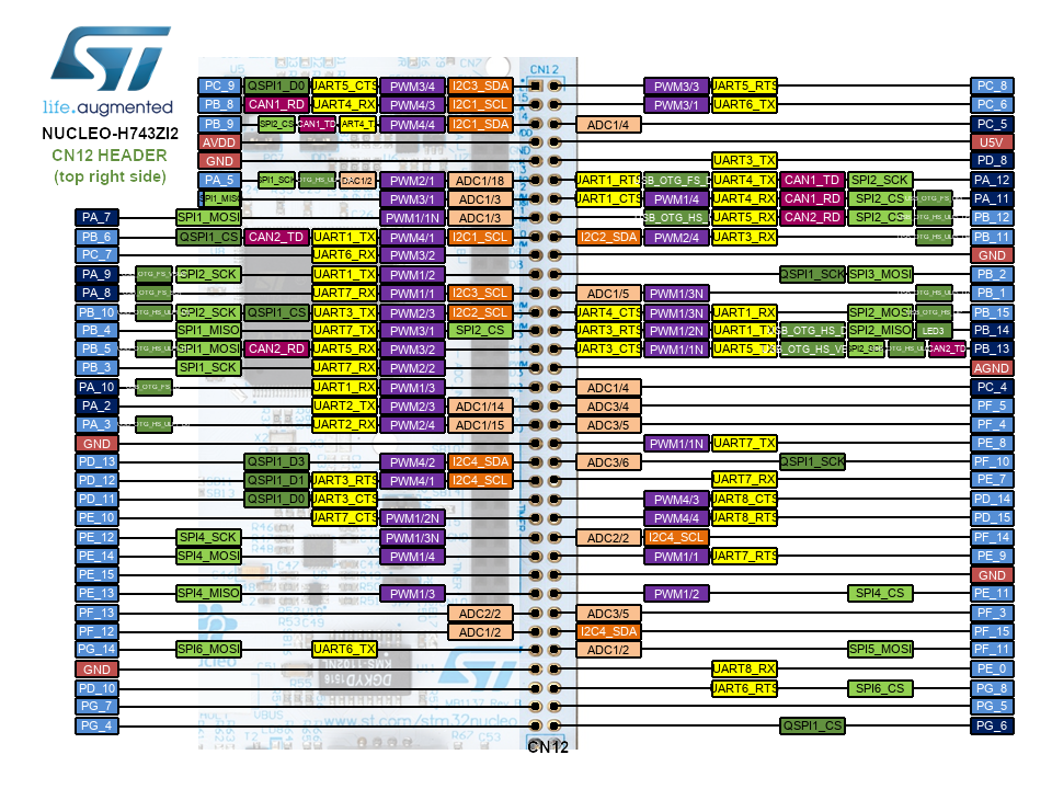
PinoutsError: (1) can't find pinout_legend_2017-06-28-2.png at /MecrispCube.MecrispCubeH743 Error: (1) can't find nucleo_h743zi2_zio_left_2019_10_9.png at /MecrispCube.MecrispCubeH743 Error: (1) can't find nucleo_h743zi2_zio_right_2019_10_9.png at /MecrispCube.MecrispCubeH743 Error: (1) can't find nucleo_h743zi2_morpho_left_2019_10_9.png at /MecrispCube.MecrispCubeH743 Error: (1) can't find nucleo_h743zi2_morpho_right_2019_10_9.png at /MecrispCube.MecrispCubeH743SCL D15, SDA D14 SCK D2, MO D4, MI D3, RX D0, TX D1The anlog pins can be used as digital pins too: A0 D16, A1 D17, A2 D18, A3 D19, A4 D20, A5 D21 Digital PinsRESET / JP1.16D0 / UART_RX / PB11 / JP1.3
D1 / UART_TX / PB10 / JP1.2
D2 /SCK / PB13 / JP1.6
D3 / MISO / PB14 / JP1.4
D4 / MOSI / PB15 / JP1.5
D5 / Button C / PC7 / JP3.10
D6 / Button B / PC6 / JP3.9
D7 / PC13D8 / PC0D9 / PB8 / JP3.8
D10 / PB9 / JP3.7
D11 / PC3 / JP3.6
D12 / PC2 / JP3.5
D13 / PC1 / JP3.4D14 / SDA / PB7 / JP3.12
D15 / SCL / PB6 / JP3.11
Analog PinsA0 / GPIO 16 / PA4 / JP1.12
A1 / GPIO 17 / PA5 / JP1.11
A2 / GPIO18 / PA6 / JP1.10
A3 / GPIO19 / PA7 / JP1.9
A4 / GPIO20 / PC4 / JP1.8
A5 / GPIO21 / PC5 / JP1.7
SD Card / SDIO PinsSDIO_D0 / SD_MISO / PC8 (internal)SDIO_D1 / PC9 (internal)SDIO_D2 / PC10 (internal)SDIO_D3 / SD_CS / PC11 (internal)SDIO_CLK / SD_CLK / PC12 (internal)SDIO_CMD / SD_MOSI / PD2 (internal)SD_DETECT / PB12 (internal)USBUSB_DP / PA12USB_DM / PA11 This work by Peter Schmid is licensed under a Creative Commons Attribution-ShareAlike 4.0 International License. | ||||||||||||||||||||||||||||||||||
View topic | History: r13 < r12 < r11 < r10 | More topic actions...
Ideas, requests, problems regarding TWiki? Send feedback