Serial EEPROMs as Mass Storage
Intro
Forth without mass storage (blocks, screens) is a not complete. A SD-Card interface could be a reasonable solution but it is an overkill for a small Forth system. Small serial EEPROMs are for my opinion more suitable.
SPI EEPROMs
SPI EEPROMs
The Serial Peripheral Interface SPICLK MC ->- host MOSI MC ->- host MISO MC -<- host SS MC ->- host or other peripherals (optional)A high-to-low transition on the CS pin is required to start an operation and a low-to-high transition is required to end an operation. Invalid Opcode: If an invalid opcode is received, no data will be shifted into AT25M02 and the Serial Data Output (SO) pin will remain in a high impedance state until the falling edge of CS is detected again. This will reinitialize the serial communication. While in Hold mode, the SO pin will be in a high impedance state. In addition, both the SI pin and the SCK pin will be ignored. From 1024 Kibit up there are 24 address bits, 8 Kibit to 512 Kibit have 16 address bits. 1, 2, and 4 Kibit have 8 bit address bits. 25LCxxxx Instruction Set
| Name | Format | Description |
|---|---|---|
| CE | 1100 0111 | Chip Erase erase all sectors in memory array |
| DPD | 1011 1001 | Deep Power-Dow |
| PE | 0100 0010 | Page Erase erase one page in memory array |
| READ | 0000 0011 | Read data from memory array beginning at selected address |
| RDSR | 0000 0101 | Read STATUS register |
| RDID | 1010 1011 | Release from Deep power-down and read electronic signature |
| WRDI | 0000 0100 | Reset the write enable latch (disable write operations) |
| SE | 1101 1000 | Sector Erase erase one sector in memory array |
| WREN | 0000 0110 | Set the write enable latch (enable write operations) |
| WRITE | 0000 0010 | Write data to memory array beginning at selected address |
| WRSR | 0000 0001 | Write STATUS register |
| Name | Format | Description |
|---|---|---|
| READ | 0000 0011 | Read from Memory Array |
| WRITE | 0000 0010 | Write to Memory Array |
| WREN | 0000 0110 | Set Write Enable Latch (WEL) |
| WRDI | 0000 0100 | Reset Write Enable Latch (WEL) |
| RDSR | 0000 0101 | Read Status Register (SR) |
| WRSR | 0000 0001 | Write Status Register (SR) |
| LPWP | 0000 1000 | Low Power Write Poll |
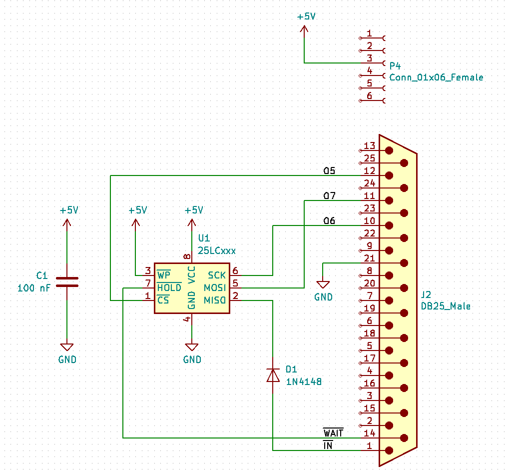
EEPROM Connected to MC's Centronics Connector (Switches and LEDs)
EEPROM Connected to MC's Centronics Connector (Switches and LEDs)
Sharing the LED and Switch port, you loose three LEDs and one switch or IN. Possible conflict with the bootstrap loader, if there is a read sequence (CS and read pattern 0000 0011). To prevent this, set the EEPROM into HOLD state e.g. with the WAIT signal.| SPI | MC (Master) | 25LCxxxx (Slave) | Interface |
|---|---|---|---|
| MISO | J2.1 IN EF4 | 2 SO | diode e.g. 1N4148 |
| MOSI | J2.11 O7 LED7 | 5 SI | direct |
| CLK | J2.10 O6 LED6 | 6 SCK | direct |
| CS | J2.12 O5 LED5 | 1 CS | direct |
| P4.3 VDD | 8 VCC | +5V capacitor 100 nF to GND | |
| " | 3 WP | +5V | |
| J2.14 WAIT | 7 HOLD | direct | |
| 21 GND | 4 GND | GND |
Read Byte
CS0     EQU     0b1101111
CS1     EQU     0b0010000
CLK0    EQU     0b1011111
CLK1    EQU     0b0100000
DATA0   EQU     0b0111111
DATA1   EQU     0b1000000

        ; MSB first

READBYTE:
        LDI     0
        PLO     R5
        LDI     0xFF
        PHI     R6
        LDI     0xFF - 8
        PLO     R6
        SEX     R0
BITLOOP:
        OUT4,0b01000000      ; CLK for SPI
        OUT4,0b00000000
        INC     R6
        GHI     R6           ; set CARRY
        SHRC
        GLO     R5
        B4      SETBIT       ; branch if bit set
        SHL                  ; bit not set
        BR      SAVEBIT
SETBIT:
        SHLC
SAVEBIT:
        PLO     R5
        GLO     R6
        BNZ     BITLOOP
about 230 cycles for one byte -> 1 ms -> 1 KiB takes about 1 s @ 1.79 MHz
Write Byte
WRITEBYTE:
        LDI     0
        PHI     R6
        LDI     8
        PLO     R6
        SEX     R0
BITLOOP:
        GLO     R5           ; get the next bit
        SHLC                 , next bit is in the carry
        PLO     R5
        BDF     SETBIT
        OUT4,0b01000000      ; CLK for SPI with data bit cleared
        OUT4,0b00000000
        BR      NEXT
SETBIT:
        OUT4,0b11000000      ; CLK for SPI with data bit set
        OUT4,0b10000000
NEXT:
        DEC     R6
        GLO     R6
        BNZ     BITLOOP
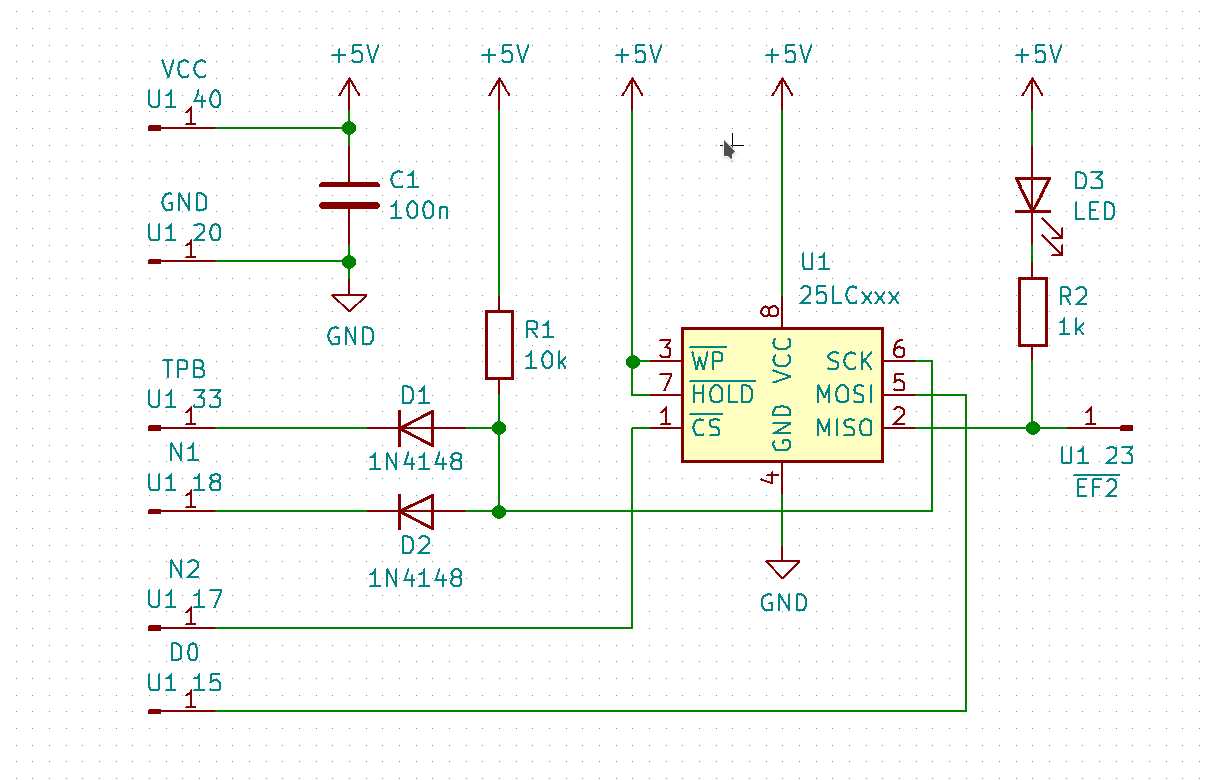
EEPROM patched on MC PCB
EEPROM patched on MC PCB
SPI Mode 0, data is always latched in on the rising edge of SCK and always output on the falling edge of SCK. For CS one output port bis is needed e.g. O7 or N2 (INP4) to start/end operation (A high-to-low transition on the CS pin is required to start an operation and a low-to-high transition is required to end an operation).| SPI | MC (Master) | 25LCxxxx (Slave) | Interface |
|---|---|---|---|
| MISO | EF2 | 2 SO | direct |
| MOSI | D0 | 5 SI | direct |
| CLK | TPB & N1 (OUT2) | 6 SCK | wired AND |
| CS | N2 | 1 CS | direct |
| 8 VCC | +5V | ||
| 3 WP | +5V | ||
| J2.14 WAIT | 7 HOLD | direct | |
| 4 GND | GND |
Read Byte
        ; MSB first

        LDI     0
        PLO     R5
        LDI     0xFF
        PHI     R6
        LDI     0xFF - 8
        PLO     R6
        SEX     R6
BITLOOP:
        OUT2                 ; CLK for SPI, INC Rx
        GHI     R6           ; set CARRY
        SHRC
        GLO     R5
        B2      SETBIT       ; branch if bit set
        SHR                  ; bit not set
        BR      SAVEBIT
SETBIT:
        SHRC
SAVEBIT:
        PLO     R5
        GLO     R6
        BNZ     BITLOOP
about 200 cycles for one byte -> 1 ms -> 1 KiB takes about 1 s
Write Byte
WRITEBYTE:
        LDI     0
        PHI     R6
        LDI     8
        PLO     R6
        SEX     R0
BITLOOP:
        GLO     R5           ; get the next bit
        SHLC                 , next bit is in the carry
        PLO     R5
        LSNF
        OUT2,0b00000000      ; CLK for SPI with data bit cleared
        LSDF
        OUT2,0b00000001      ; CLK for SPI with data bit set
        DEC     R6
        GLO     R6
        BNZ     BITLOOP
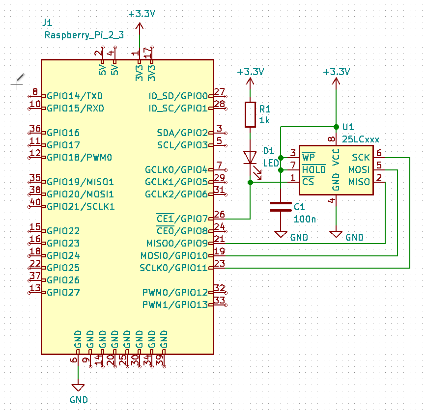
EEPROM Connected to Raspberry Pi
EEPROM Connected to Raspberry Pi
- http://www.netzmafia.de/skripten/hardware/RasPi/RasPi_SPI.html
- https://www.raspberrypi.org/documentation/hardware/raspberrypi/spi/README.md
- http://wiringpi.com/reference/spi-library/
| SPI Function | BCM/GPIO | RaspiElf |
|---|---|---|
| SPI0 MISO | 9 | IN4 |
| SPI0 MOSI | 10 | IN3 |
| SPI0 SCLK | 11 | IN6 |
| SPI0 CS0 | 8 | IN7 |
| SPI0 CS1 | 7 | O0 |
| EEPROM CS | 5 | O1 |
| SPI1 MISO | 19 | O5 |
| SPI1 MOSI | 20 | - |
| SPI1 SCLK | 21 | shutdown |
| SPI1 CS0 | 18 | CLR |
| SPI1 CS1 | 17 | WAIT |

eeprom2bin (download tool)
- NAME
- eeprom2bin - Copies the EEPROM memory to a binary file on the Raspberry Pi.
- SYNOPSIS
- eeprom2bin [-s hexadr] [-e hexadr] [file]
- DESCRIPTION
- Copies the EEPROM memory to a binary file (or stdout) on the Raspberry Pi. The Raspberry Pi GPIO SPI0.1 is used as interface to the SPI EEPROM (24 bit address, at least a 1024 Kibit type, 256 byte page). The generated data is written to the standard output stream or to a file. Caution: Overwrite file if it exists. Use > for redirecting (save the file) or | for piping to another command (e.g. hexdump).
- OPTIONS
- Non argument options that are duplicated on the command line are not harmful. For options that require an argument, each duplication will override the previous argument value.
- -s hexadr
- start address in hex (0 is default)
- -e hexadr
- end adress in hex (0x1FFFF is default)
bin2eeprom (upload tool)
- NAME
- bin2eeprom - Copies the content of binary file on the Raspberry Pi to EEPROM.
- SYNOPSIS
- bin2eeprom [-s hexadr] [-e hexadr] [file]
- DESCRIPTION
- Copies the content of binary file on the Raspberry Pi to EEPROM memory. The Raspberry Pi GPIO SPI0.1 is used as interface to the SPI EEPROM (24 bit address, at least a 1024 Kibit type, 256 byte page). Use < for redirecting or | for piping from another command.
- OPTIONS
- Non argument options that are duplicated on the command line are not harmful. For options that require an argument, each duplication will override the previous argument value.
- -s hexadr
- start address in hex (0 is default)
- -e hexadr
- end adress in hex (0x1FFFF is default)
Kermit/ZModem
Kermit/ZModem
What about using KERMIT or ZMODEM protocol for the file transfer and use the file system on the host? No need to add additional hardware (SD-card is anyway to modern You could use an old CP/M or even a PDP11 as host. The C-Kermit Local Server mode, e.g. MC can read/write the blocks as files
 block.0, block.2, block.255.
The serial communication is really slow, not only because of the 9600 baud, but you have to wait after each character to give CDP1802 some computation time.
https://github.com/utoh/pygmy-forth/blob/master/extras/kermit/pfkerm.docComments


| I | Attachment | History | Action | Size | Date | Who | Comment |
|---|---|---|---|---|---|---|---|
| |
raspi-eeprom.png | r2 r1 | manage | 25.0 K | 2019-01-26 - 20:36 | PeterSchmid |
Topic revision: r6 - 2019-01-27 - PeterSchmid

 |
|
|
Ideas, requests, problems regarding TWiki? Send feedback